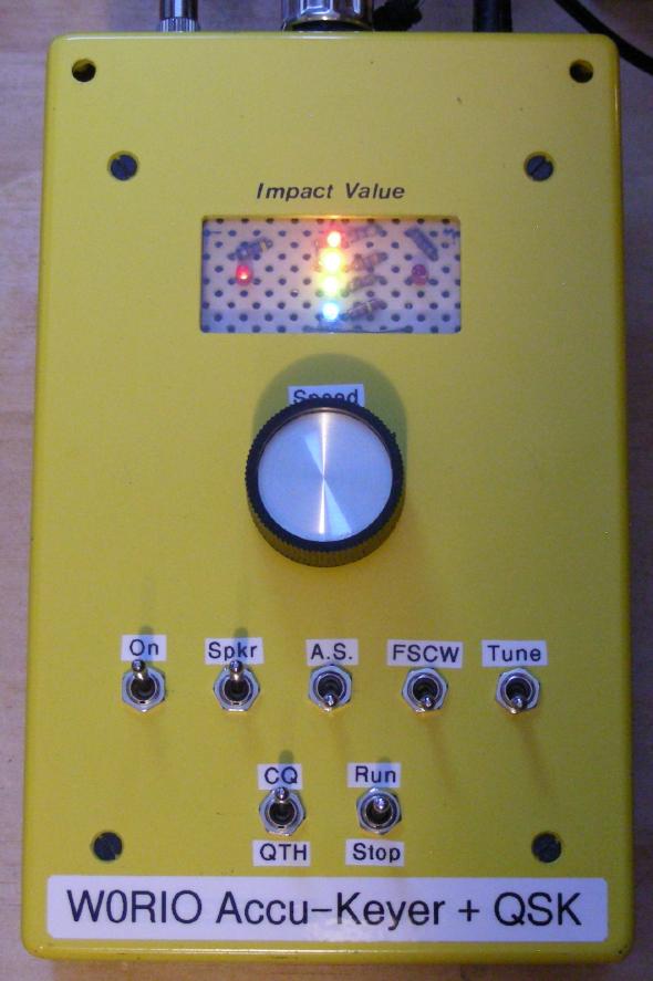
Front view of the Accu-Keyer Extended, the LEDs turn on while sending
(C) 2021, G. Forrest Cook W0RIO
Front view of the Accu-Keyer Extended, the LEDs turn on while sending
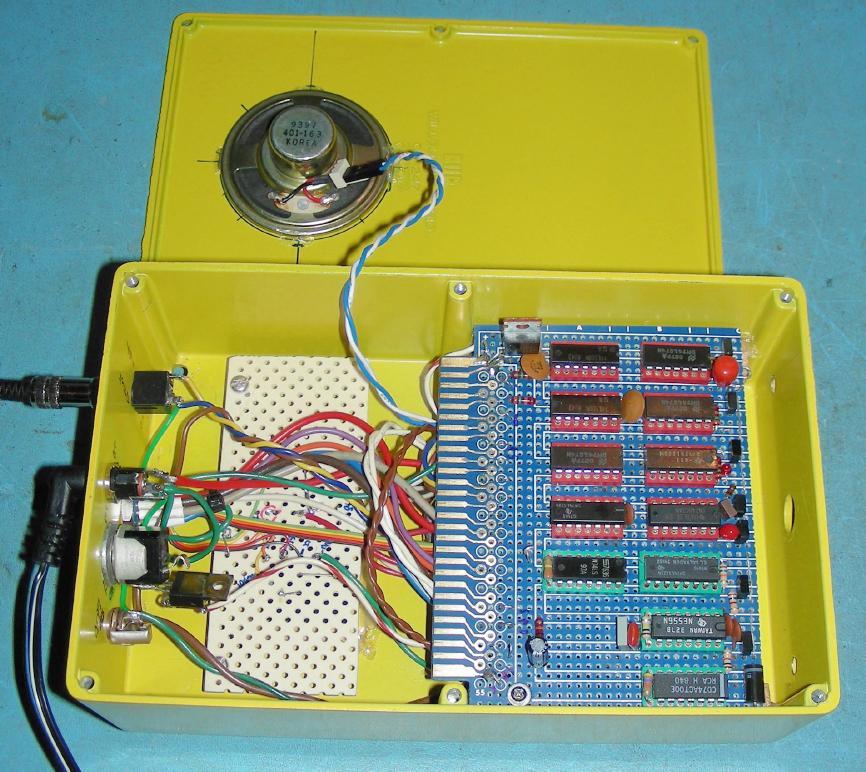
Inside view of the Accu-Keyer Extended before adding the Memory Keyer board
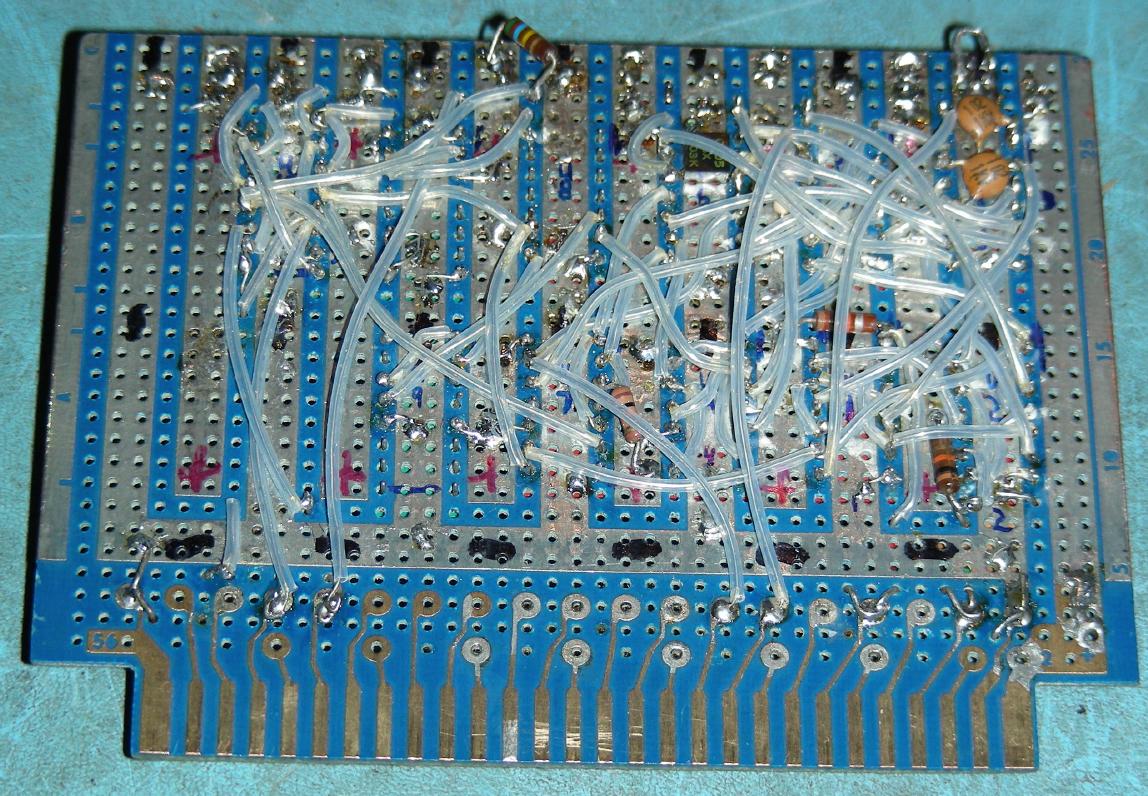
The Accu-Keyer Extended hand-wired circuit board before completion
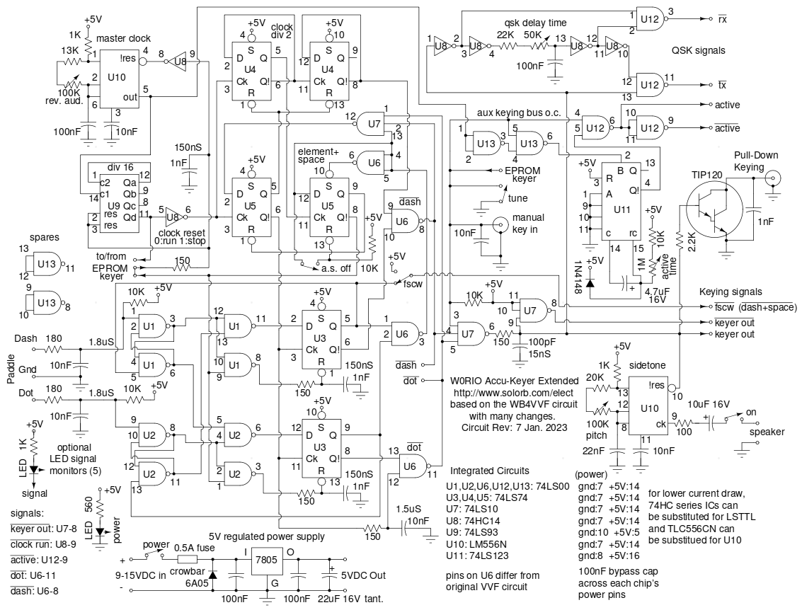
Schematic of the Accu-Keyer Extended QSK keyer
This project is an extended version of the 1973 WW4VVF Accu-Keyer, an automatic type B iambic Morse code keying device. The Accu-Keyer has been time-tested and is known for being a great keyer. This version adds several features to the original circuit including time-sequenced outputs for a full break-in QSK system and support for experimental two-tone frequency shifting CW (FSCW) transmitters. It also includes a 5 color LED array that puts on a light show when the keyer is sending code. I use my Spatula Paddle with this keyer, the two projects combine to to make sending Morse code a pleasurable experience.
Many people may ask why go to all of the trouble of wiring up a dozen TTL chips to make a keyer when there are many PIC and Atmel based keyers that can be purchased for under $10. First, there's a nostalgia element to this project. A 45+ year old TTL project is not that different from a 50+ year old vacuum tube project.
Second, this keyer features extremely low-latency timing, which makes for very accurate Morse character generation. Software-based keyers can add small delays between sensing the paddle inputs and producing an output pulse. Finally, having access to the internal logic signals allows for experimentation with ideas like frequency-shifting CW and playing with blinky LEDs.
The original Accu-Keyer was known for sometimes having timing problems when the first element sent was a dit, this version fixes this problem by adding R-C delays inline with several of the critical signals and a higher speeed clock combined with a divider chip. Other improvements have been made to the original circuit including the addition of bypass capacitors to the keyer input lines and "beefing up" the pull-down keying circuit so that it can drive higher current loads. The original circuit had a few floating input lines on the flip-flops, these have been tied to the +5V rail for better RF immunity and compatibility with CMOS logic chips.
The majority of the circuitry is very close to the original Accu-Keyer circuit, with the exception that the logic family was changed from regular 74xx TTL chips to lower power 74LSxx TTL. It was later changed to 74HCxx CMOS chips for even lower power consumption. The original WB4VVF article explains the circuit operation in detail, see the link below.
A few changes were made to the original logic circuitry, mostly to remove some unwanted glitches. In the WB4VVF circuit, U3 pin 1 had a small RC time delay circuit on the dash memory reset pin, an equivalent delay circuit was added to U3 pin 13, the dot memory reset pin. While prototyping the circuit on a plug-board with long wires, there were problems with the circuit occasionally sending an extra first dot. This was tracked down to a race condition between U3 pin 11 (clock) and U6 pins 12 and 13, a small RC delay was added to U6 pin 12 to solve this problem.
Another glitch was found in the clock reset line, this caused the first dot to be too short, it was solved by adding another RC delay to this line. The main keyer out line also had a small glitch that showed up when sending dashes, it was noticed when connecting a TTL counter to the output line. This glitch was snubbed out with a 15nS RC network.
The master clock section has been completely reworked from the original transistor-based circuit. Numerous articles have raised concerns about the start-up character of the original oscillator. Replacing the oscillator with a 555 timer changes the start-up problem but does not really fix it. The first pulse on a 555 timer takes longer than the following pulses since the timing capacitor has to change from 0V to 2/3 VCC while the following pulses alternate between 1/3 VCC and 2/3 VCC.
The longer first pulse problem was fixed by speeding the clock up by a factor of 16 and adding a 74LS93 ripple counter to divide the faster clock by 16. This greatly reduces the longer first pulse error since it now only affects the first of 16 clock pulses, this makes the error imperceptible. Note that in the original circuit as well as this version, the clock only runs when sending, this prevents any TTL switching noise from interfering with your receiver.
A QSK circuit has been added to create the !rx, !tx signals and the active signal. The !rx and !tx signals add small delays around the dits and dots which allow for quick switching between a transmitter and receiver. See the All-Ears article below for a more detailed explanation of the QSK timing signals.
The !dash+space signal has been brought out for experimental use with frequency-shifting CW transmitters. This is used to slightly lower the frequency of a DDS VFO when a dash is being sent. See the FSCW article below for details.
The pull-down keying circuit has been changed to use a TIP120 darlington transistor, this reduces the loading on the keyer out signal while providing high current switching capabilities. Other darlington transistors can be used here.
The 5V regulated power supply features a 6A05 diode and a 0.5A fuse in a crowbar circuit for protection against reverse input voltage. The regulator output is bypassed with a 22uF tantalum capacitor and 100nF capacitors have been added across the power input pins of all of the logic chips. The circuit will work fine with a few less bypass capacitors but overkill is never a bad idea in an RF environment.
The keyer was built into a surplus Bud cast aluminum utility box that was purchased for $1 at a local recycled building materials store. It used to be a broken Clegg soil impact tester. The box already had a clear plastic window that was useful for the LED display, holes were drilled for the various switches, jacks and speaker.
The majority of the circuitry for this project was built on a perforated prototyping circuit board. The board was half of an old STD-bus prototype card that was left over from another project, it had alternating ground and +5V bus lines printed on the bottom side. IC numbers were written in indelible ink on the on the bottom of the circuit board.
All of the wiring was hand-wired and soldered, using bare 26 gauge tinned hookup wire. A small loop was added to the end of each wire, sized to fit over the IC socket pins. Connections from the 12 IC sockets to the ground and +5V bus lines on the proto board were added first, using short pieces of wire. Hard-wired input pins were also connected to the appropriate buses. The rest of the wiring was routed through pieces of teflon tubing. Teflon tubing does not melt when it is touched with a soldering iron, so it is easy to add new wires without damaging the existing ones. Wire-wrap wire could also be used here.
Most of the fixed resistors and capacitors were mounted on the spare holes in the prototype board, a few of the timing resistors were mounted in extra pins on the IC sockets so that they could be easily changed. These resistors are used in place of the active time and qsk delay time variable resistors that are shown in the schematic.
All of the optional LEDs were mounted on a separate piece of perforated circuit board which was mounted so that the LEDs were visible from the front of the box. Five colors of LEDs were used to make a nice looking display: blue for power, green for active, yellow for element+space, red-orange for keyer out and deep red for both dot and dash.
After the circuit board was built and tested, it was installed in the Bud box and hand-wired connections were added between the board and the various switches and connectors. The LED board was added after the rest of the wiring was complete and tested. All of the LED signal connections were wired between the boards using one piece of ribbon cable.
The 100K audio-taper speed control potentiometer wired to go faster as the knob is turned to the left. If you can find (or want to pay for) a 100K log-taper potentiometer, it can be wired the other way. A large round knob should be used for accurate speed control.
All of the QSK signals, the FSCW signal, ground and +5V power were wired to an Amphenol 9 pin connector on the rear of the Bud box. This connector is pin-compatible with your author's original Accu-Keyer box which also has the QSK and FSCW extensions. A more common DE9-S 9 pin D connector could be used as a substitute for the Amphenol connector.
It is possible to connect an EPROM-based memory keyer extension to the Accu-Keyer Extended circuit. A 2716 2Kx8 EPROM was used, it was programmed with two selectable messages, a CQ sequence and a QTH/Name message. The circuit has much in common with my earlier Beacon Keyer project, but this version interfaces with the clock and output logic from the Accu-Keyer Extended project.
The cw2hex program used in the Beacon Keyer project can be used to encode the two Morse messages into an Intel Hex file which which can then be used to program the 2716 EPROM. Be sure to start each message with a 1 bit space and separate the messages with a block fill, both of these functions can be done with cw2hex.
Connecting the memory keyer to the Accu-Keyer is simple. The memory keyer clock start/stop circuit is inserted in the middle of the Accu-Keyer clock reset line and the memory keyer's clock is tied to the Accu-Keyer clock signal. The memory keyer's output is tied to the Accu-Keyer aux keying open collector bus via a 2N3904 pull-down transistor. The +5V and ground power rails are also connected to the Accu-Keyer power rails.
The memory keyer circuit consists of the start/stop logic section, the address counter and the message EPROM memory. When the circuit is started, the counter counts up and the Morse Code message comes out of the EPROM D0 output. At the end of the message, the EPROM D3 output goes high which causes the clock to stop and the address counter to reset. Either of two messages are selected by sending a low or high logic level to the highest address pin on the EPROM.
Tiny glitches will show up on the EPROM output lines due to delays in the 4040 ripple counter outputs and delays within the EPROM. These glitches are removed by the small RC networks on the output pins. The circuit can support larger EPROMs to allow for longer messages or more than two messages. The extra address lines will need to be connected to the two unused address counter outputs and/or more message select switches.
Using the memory keyer is easy, just select either of the two messages and push the momentary start/stop switch to the start position. The message will be sent at the same speed as the Accu-Keyer paddles. The message will stop automatically after it has completed, it can also be interrupted by pushing the start/stop switch to the stop position or by tapping either the dot or dash paddle on the Accu-Keyer.
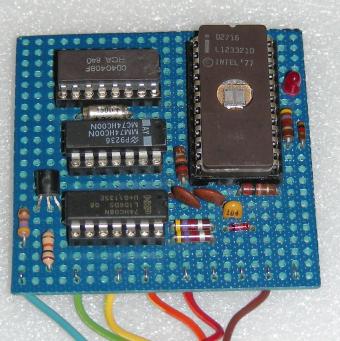
Accu-Keyer EPROM Memory Keyer circuit board
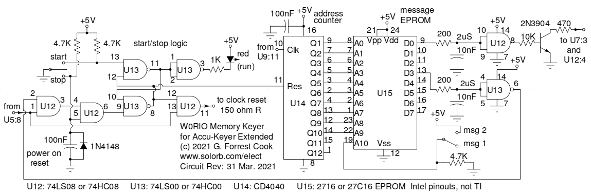
Schematic of the Accu-Keyer EPROM Memory Keyer
The Accu-Keyer Extended circuit was originally built with 74LSXX series TTL chips (Low Power Schottky) with the exception of the 74HC14, which is required for the correct QSK signal timing. With LS TTL chips, the five status LEDs and one power LED, the circuit draws around 71mA when idle and 92mA when sending continuous dashes.
It is possible to replace all of the LS TTL chips in the keyer and the memory keyer with the equivalent HC (High Speed CMOS) chips. This family of chips draw considerably less current and is recommended if battery operation is planned. The 556 dual timer IC can also be replaced with a TLC556CN, which is a lower power CMOS part. For more power savings, most or all of the LEDs can be left out of the circuit, or an LED disable switch can be added between the LED board's +5V line and the LED anode pins. Using all HC chips, a 27C16 CMOS Eprom and just one LED for a power indicator, the entire circuit draws 20mA idle and 25mA when active. The final version of this project is now using all HC and CMOS chips.
Back to FC's Ham Radio Circuits page.