(C) 2020, G. Forrest Cook, W0RIO
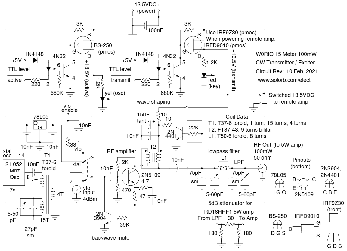
This 100mW QRPp transmitter project was put together after your author acquired a surplus 21.052 Mhz TTL oscillator module. That frequency is within the 15 Meter (21 Mhz) ham radio band's Morse Code segment, so the oscillator was a perfect candidate for a simple CW transmitter. The transmitter has a wave-shaped envelope which produces a click-free sound. The oscillator is automatically stopped and started by a signal from the external keyer, this eliminate chirps. A back-wave attenuator circuit is used to reduce the oscillator leak-through signal during key-up times. Harmonic radiation is around 40dB below the carrier, which is considered clean at the 100mW power level.
In short, the transmitter outputs a small, but very well-formed CW signal. To be exact, this is a QRPp transmitter since the output is below 1W. The transmitter is controlled by my modular QSK CW system, which supports several different homebrew transmitters. Fully manual operation can also be easily accomplished by connecting a transmit switch and a key signal to the control inputs. The circuit can be used as an exciter for driving a higher power RF amplifier and an external VFO input is provided to allow the transmitter to operate on different frequencies.
This transmitter is well-suited for short-range morse code communication such as talking to nearby hams. If propagation conditions are favorable and an efficient antenna is used, the transmitter can be heard for hundreds of miles.
The heart of the transmitter is the 21.052Mhz crystal oscillator module. The module produces a square wave signal. The oscillator output is DC-bypassed by a 10nF capacitor which feeds a single turn input loop on the oscillator transformer. The 15 turn oscillator transformer link is wired across a fixed and a variable capacitor to produce a resonant circuit at 21Mhz. The 4 turn output link is used to match the impedance of the 2N5109 RF amplifier.
The 2N5109 circuit is a copy of the W8DIZ (kitsandparts.com) 20dB amplifier kit, a few capacitor values have been changed. The amplifier produces a 7V peak-to-peak signal across a 50 ohm load, or just above 100mW.
The RF amp's signal is passed through a simple lowpass filter to the output. The filter reduces the level of the harmonics from the signal to prevent interference to users of higher frequencies. The output level after the filter is just around 100mW.
The !active (oscillator enable) and ~transmit (keying) signals drive the LEDs on a pair of 4N32 opto-isolators. The 1N4148 diodes make sure the opto-isolator turns fully off if true TTL logic is used. The 220 ohm resistors provide current limiting for the isolator LEDs. The base of the opto-isolator transistors are pulled down with a 680K resistor to prevent false triggering.
The opto-isolator transistors pull the 13.8VDC signal down through a 3K resistor to produce the inverted gate drive signal for the PMOS fet transistors. The Drain pin of the pmos fets switch the +13.8VDC power to the oscillator and amplifier circuits, with very little loss. Nearly any PMOS transistor rated to pass a few hundred milliamps or more should work in this circuit. If an external amplifier is switched in parallel with the 2N5109 amplifier stage, the IRFD9010 PMOS fet keying transistor should be replaced with a higher current device such as an IRF9Z30 type to reduce resistive losses in the amp's power supply line.
The switched 13.8V active signal powers a 78L05 5V regulator IC, which in turn powers the oscillator module and the yellow osc LED circuit.
The switched 13.8V transmit signal provides power to the amplifier stage through a wave shaping circuit consisting of a 10 ohm series resistor and a 15uF tantalum capacitor. That rounds the rising edge of the keyed amplifier waveform. The signal also powers the red key LED circuit. The 2N4401 transistor uses the inverted transmit signal from the opto-isolator to discharge the 15uF capacitor through a 10 ohm resistor during key-up times. That rounds the falling edge of the keyed amplifier waveform.
The inverted transmit signal is also used to activate the 2N3904 Back-wave muting transistor. This greatly reduces the back wave RF that leaks from the oscillator through the amplifier circuit during key-up times.
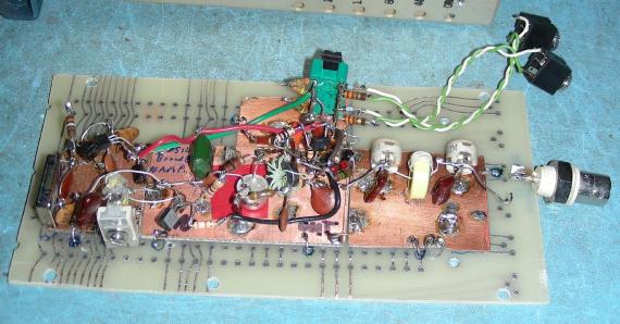
The input isolators, oscillator, RF Amp and lowpass output stages were built on several small squares of bare copper circuit board material using the ugly or dead bug construction method. The small boards were then connected to a spare piece of printed circuit board material, which acts a a substrate. Small soldered wire bridges were used to connect the various boards together and connect the boards to the substrate. Grounded components were soldered directly to the copper boards and some of the larger components were secured to the board using hot-glue.
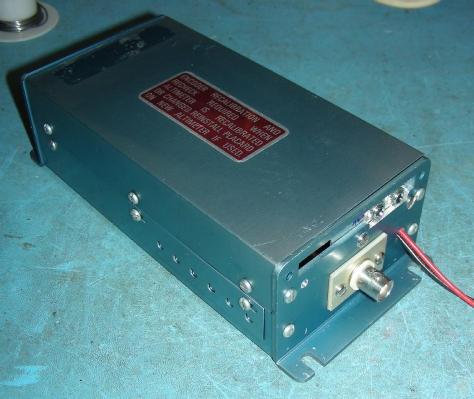
The substrate board was mounted inside of a surplus aluminum box. The keying signals, and RF output signal and DC power input were all run through the back of the box. Stereo 3.5MM audio jacks were used for the keying signals, the ground pin is unused, the tip pin connects to +5V and the ring pin connects to the TTL level keying signal. A BNC jack was used for the RF output. The Oscillator and Keying LEDs were mounted in small holes on the front of the box and secured with hot-glue.
The RF output should be connected to a 50 ohm dummy load, a 50 ohm, 1/2W carbon resistor will work fine. 13.8VDC power should be connected to the DC input and appropriate keying signals should be connected to the inputs. The keying signals can be produced by connecting an external 5V power supply between the +5V, !active and !transmit inputs.
Connect an oscilloscope across the 4 turn output link on the T37-6 oscillator toroid. Activate the !active signal. Adjust the scope so that it shows a 21Mhz wave. Adjust the 5-50pF oscillator trimmer capacitor for the largest sine wave signal on the oscilloscope.
Connect the oscilloscope across the RF output's dummy load. Activate both the !active and !transmit signals. Adjust the two lowpass filter variable capacitors for the largest and most pure looking sine wave. Re-adjust the oscillator's trimmer for the largest pure looking sine wave. Repeat the lowpass filter adjustments. Increase the output capacitor's value slightly so that the output level just starts to drop, this is where the lowpass filter starts to greatly reduce the harmonics. A spectrum analyzer can also be used to adjust the lowpass filter, but it is not required.
Your author just needs to connect the transmitter control signals and RF output to the aforementioned modular QSK CW system. This system controls the antenna switching and receiver muting/AGC timing functions. I use an antenna tuner feeding a 40 meter dipole, the tuner is adjusted for the lowest SWR.
A manually controlled T/R switch can be used for the !active signal and antenna switching. A manual key or electronic keyer can drive the !transmit line. A simple 21.05 Mhz dipole can be constructed with two 11'-1" bare wires and a short piece of 50 or 75 ohm coaxial wire. The dipole should be hung free and clear of any nearby objects.
An external RF amplifier is a good addition to this project. The RD16HHF1 MOSFET amplifier from my 28Mhz Beacon has been used with this transmitter to boost the output power to around 5W. The only modifications required were the addition of a 5dB attenuator pad between this transmitter's lowpass filter and the external amp's input, and the IRFD9010 pmos transistor was changed to a lower resistance IRF9Z30 type. The amp's existing 28 Mhz lowpass filter was sufficient to produce a 3rd harmonic level of -43 dB on 21 Mhz, a 21 Mhz lowpass filter would reduce the harmonics even further.
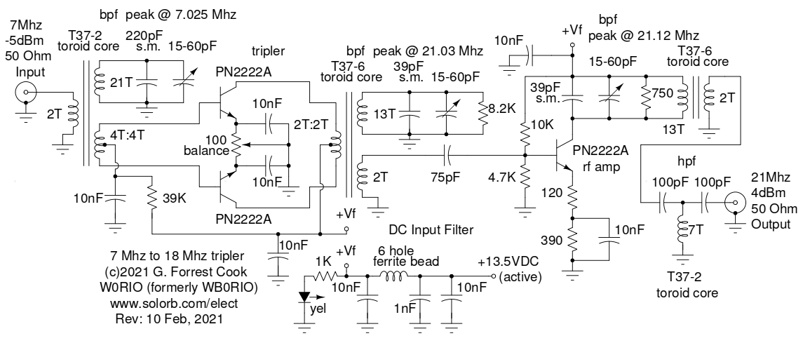
An external VFO (variable frequency oscillator) input was added to allow the transmitter to tune across the CW portion of the 21 meter band. The DDS VFO used is only capable of operating up to 8 Mhz, so a tripler circuit (shown above) was built for converting the 7Mhz VFO signal to 21Mhz.
The tripler circuit uses a 7 Mhz input filter and a 21 Mhz output filter followed by a tuned RF amplifier. It is powered by the transmitter's vfo enable output. A Tee highpass filter was added to the tripler output to reduce the level of the 7 and 14 Mhz sub-harmonics, which can pass through the rest of the transmitter circuitry. The three resonant circuits in the tripler are tuned to slightly different base and harmonic frequencies to provide a broader pass-band. Resistors across the two 21Mhz resonant circuits also broaden the pass-band.
Back to FC's Ham Radio Circuits page.