(C) 2011, G. Forrest Cook, W0RIO (formerly WB0RIO)
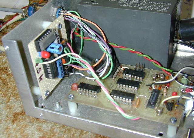
The QSK timing generator next to an original WB4VVF Accu-keyer board

In the world of amateur (ham) radio Morse code communications, QSK refers to a method of operation where the transmitter and receiver are alternately active when the key is down or up. QSK is also known as full break-in keying. QSK operation allows the operator to hear what is happening on their frequency in the brief times between transmitting Morse code dits and dahs. The conversation can be quickly interrupted by the other station, or by a third station. The sender also knows immediately if their signal is being interfered with, allowing for re-transmission of the interfered parts of the outgoing message.
The design of a QSK-capable radio station is somewhat tricky. A QSK system has to quickly switch the antenna between the transmitter and receiver, key the transmitter, mute the receiver during transmission and disable or shift the transmitter's oscillator during receiving. It is also desirable to change the receiver's AGC response time from fast to slow when not transmitting to smooth out the choppy sound of fast AGC. By adding small delays at the beginning and ending of the dots and dashes, it is possible to generate signals with slightly longer and shorter lengths compared the original Morse code. These modified signals sequence the entire system in order to eliminate transmitted chirps, T/R relay arcing and receiver clicking noises.
Here's a typical sequence for sending one Morse code "dit", items in parentheses happen simultaneously: (key down: antenna relay to transmit, transmitter oscillator on, receiver mute), [delay], (transmitter output on for duration of dit), (key up: transmitter output off), [delay], (antenna relay to receive, transmitter oscillator off, receiver unmute). Additionally, the receiver AGC slow/fast signal needs to switch to fast at the beginning of the the first key down event, and should switch to slow a few seconds after the last key up event.
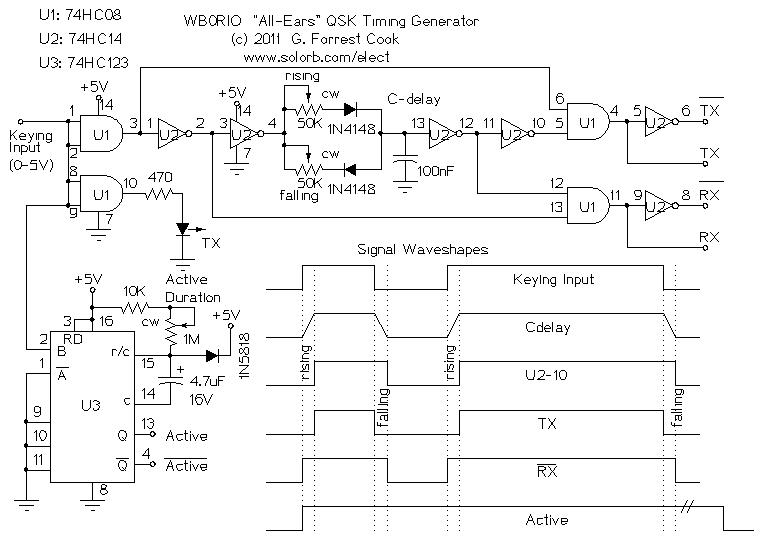
This circuit takes a 5VDC keying signal and produces three 5VDC output signals as well as inverted versions of the three signals. This combination of outputs is useful for driving a variety of control circuits that can interface to the transmitter and receiver. The timing generator also produces the necessary signals for automatic non-QSK transmit/receive switching.
See the Modular CW Transmitter Prototyping System article to see how this circuit can be connected to a receiver, transmitters and related devices. A variation of the QSK timing generator circuit has been included in my Accu-Keyer Extended keyer and is implemented in software in my Arduino-based Simpler is Better Keyer.
The logic family selected for this project was 74HC (high speed CMOS). This is a relatively modern and low power family of ICs. The circuit should work with other CMOS logic types such as the 4000 series. Note that a 74LS14 chip should not be used as a replacement for the 74HC14 since it is not compatible with the delay timing circuit.
The main considerations for the selected logic family are power consumption and compatibility with the the output of your keyer. Note that 74XX and 74LSXX TTL output signals typically swing between 0V to 0.4V (low) and 2.4V to 5V (high) while 74HCXX CMOS output signals swing very close to the 0V and 5V "rails". The 74HCXX chips in this project may not work properly when driven by signals from 7400 or 74LS00 series TTL ICs. A 74HCT buffer stage can be used to convert a TTL level keyer output to the HC levels used by this circuit.
The external keying input drives three inputs, the timing chain buffer (U1 pins 1,2), the TX LED buffer (U1 pins 8,9) and the Active timer U3. The first two section of U2 produce inverted and non-inverted versions of the keying signal for use down the line. The non-inverted keying signal drives the resistor/diode/capacitor delay circuit. The separate rising and falling controls are used to adjust the rising and falling delays independently. This is an optional feature, for equal rise/fall times a single 50K pot between U2 pins 4 and 13 can replace the two 50K trimpots and associated diodes. Rise and fall delays of around 5mS should be a good starting point.
The output of the delay circuit is squared by the next section of U2 and inverted. The inverted delayed signal is inverted again by the fourth section of U2. The keying signal and delayed keying signal (inverted and non-inverted) are combined in the two remaining U1 and gate sections to produce the TX and RX! signals, these two signals are inverted by the last two sections of U2 to produce TX! and RX.
The Active and Active! signals are produced by one-shot U3, the active duration control is set so that the active line stays high for several seconds after transmission has ended. The 1N5818 diode on the 74HC123 r/c input is recommended by some IC manufacturers to protect the chip from back-fed timing capacitor voltage on power-down.
Note that half of a dual monostable multivibrator 74HC123 part was used in this circuit since the chip is a retriggerable device. A single monostable multivibrator such as the 74HC121 will not work here since it is not retriggerable and will produce a "glitchy" output signal. A 74HC122 single retriggerable monostable multivibrator could probably be used but it is a fairly rare part.
The six outputs can be used to drive a variety of control circuits on the transmitter and receiver. Normally, only the inverted transmit and receive lines and the Active lines are used for the QSK system. I recommend using the signals to drive opto-couplers inside of the transmitter and receiver where possible, current limiting resistors should be used between the outputs and the opto-coupler LEDs.
The output signals use common stereo 3.5mm jacks and plugs. The "ground" or "sleeve" side of the jacks are left floating to eliminate any ground loops. The jacks should be mounted to their respective chassis via insulating washers. If the jacks have to be mounted to to the chassis, the shield lines should be disconnected on the plug end of the wiring.
Note that the tip of the 3.5MM plugs have +5VDC on them and should only be connected or disconnected when the 5V power supply is turned off. They can produce a spark if they contact a grounded chassis. Other types of plugs and jacks such as DIN or DE9 types may be preferable if you need to "hot swap" these signals. As long as your 5VDC supply is current-limited to a reasonable level, such as 1 amp or lower, there should not be any significant risk of problems. A high-amperage 5VDC supply should not be used to power this circuitry and a 500mA fuse would be a good thing to have in series with the +5VDC supply line.
A fast-acting reed relay is used for the antenna T/R switch. If you can find one, a mercury-wetted reed relay is a good choice for the antenna relay. A second reed relay is used in the T/R switch to short the receiver input to ground while transmitting, this prevents receiver overload. A third reed relay is driven by the Active signal to switch a receiver's AGC circuit between fast AGC (transmitting) and slow AGC (receiving). The T/R relay and AGC relays are driven by a standard NPN transistor relay driver circuit.
Don't forget the backwards diode across the relay coil, it protects the driver transistor from the reverse high voltage inductive spike that happens when the relay coil is turned off. A subtle variation on the snubber diode circuit involves adding a 24V zener diode in series with the regular silicon diode, this can speed up the relay's hang time when the coil is de-energized. The cathode of the Zener should be pointed in the opposite direction as the normal snubber diode.
An optional addition to the circuit is a switched ballast control for a vacuum tube power supply. The !Active signal controls an optically-isolated MOSFET switch that puts a load across the high voltage line of the power supply when the transmitter is active. This has the effect of regulating the high voltage supply in order to "flatten" out the envelope of the transmitted dots and dashes.
This circuit was built inside of the metal box that houses my antique WB4VVF Accu-Keyer circuit board and a 5V power supply. The circuit was constructed on a small piece of perforated circuit board using IC sockets and point-to-point wiring. A solderable prototype circuit board would also be a good platform for construction. Bypass capacitors are not shown in the schematic, One 100nF capacitor should be placed across the VDD (+5V) and VSS (ground) pins on every IC and one 47uF 16V capacitor should be wired between +5V and ground. The six output signals were connected to a 9 pin connector connector along with +5V and ground.
The various outputs and 5V DC power from the timing generator are routed from the 9 pin connector through a shielded wire and to an external junction box that is called the starfish hub. The relay driver circuits were built into the junction box. Since the circuit will be used in an environment with a lot of stray radio frequency (RF) energy, shielded wires should be used for all external connections. Only connect the shields to ground on one side to prevent ground loops.
Connect a dual-trace oscilloscope to the TX and RX signals, then send a stream of Morse code "dit" characters and adjust the rising and falling controls for the desired delays. Another method is to connect everything up and adjust the delays for the minimum amount of clicking. Proper adjustment is largely a function of your specific transmitter and receiver's timing characteristics.
Adjust the Active Duration control for desired operation of your receiver's AGC function and the transmitter's power supply ballast load if it is implemented. It may be useful to use a panel-mounted potentiometer for the Active Duration control so that it can be adjusted during station operation, although your author has not found this to be necessary.
This circuit has mainly been used with a Drake 2B receiver and several different vacuum tube transmitters. The Drake 2B AGC switch should be set to the "Fast" mode during operation. The interface circuit adds 220nF of capacitance across the receiver's AGC line during transmission (ACT) or 1uF across the AGC line during receive. The circuit has also been used with a National NC-155 receiver.
Once the QSK system is up and running, operation is completely automatic. Just use the keyer paddles or manual key to switch from receive to transmit and back. Operating a station with QSK capabilities makes having a Morse code conversation feel much more interactive, especially if the operator on the other side also has QSK capabilities.
Back to FC's Ham Radio Circuits page.